Key Takeaways & Executive Findings
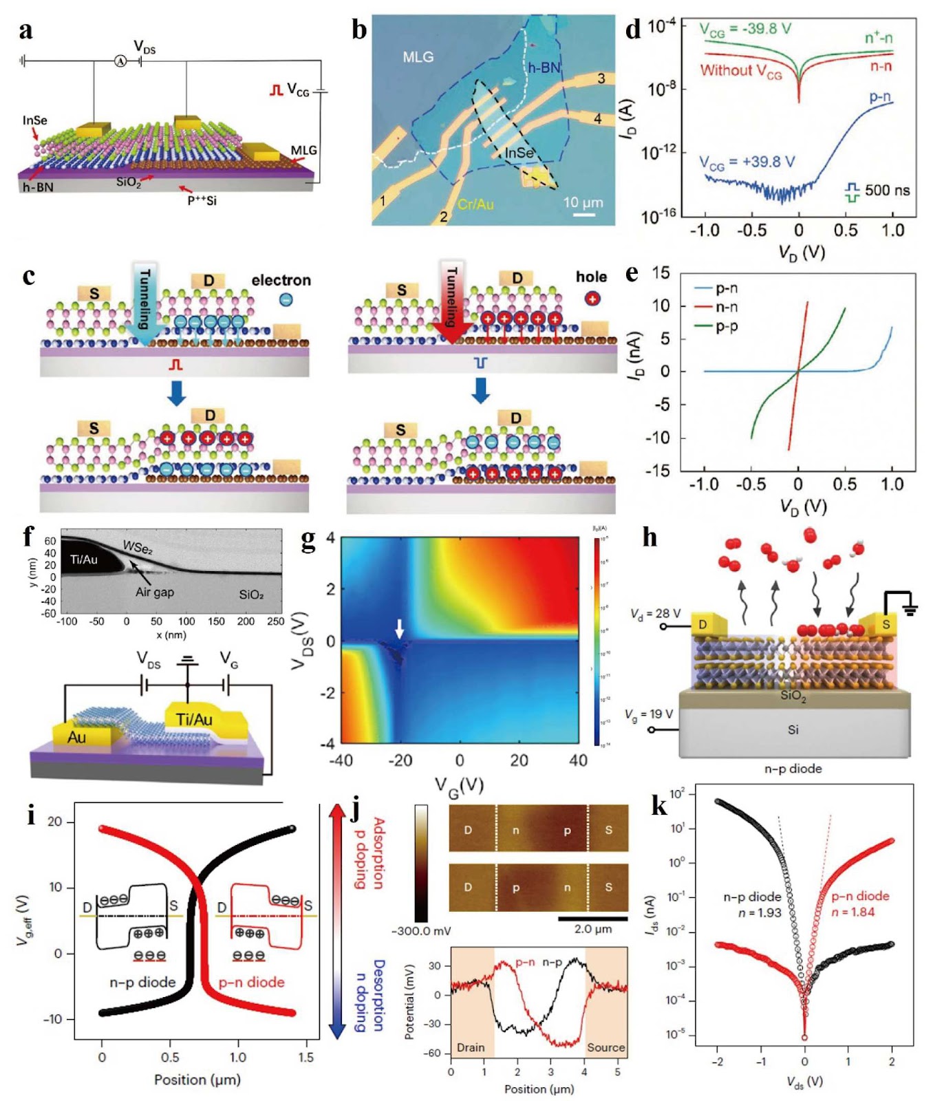
- •• • Reconfigurable photo-induced doping in 2D van der Waals semiconductors enables dynamic polarity control with switching speeds below 1 ms, as demonstrated in Nat Electron (2020), directly addressing the fixed carrier type limitation of silicon CMOS. • • Anti-ambipolar heterojunctions of GeAs and SnS2 achieve multi-logic state operation with peak-to-valley current ratios exceeding 10^3 at room temperature, providing a route to multivalued logic circuits with reduced transistor count (Appl Phys Lett, 2024). • • Non-volatile neuromorphic photovoltaics based on reconfigurable 2D materials exhibit retention times >10^4 s and endurance >10^3 cycles, enabling energy-efficient image processing with in-sensor computing (Nat Nanotechnol, 2023). • • Multi-valued logic transistors using ZnO composite nanolayers with mobility edge quantization demonstrate three distinct logic states with static power consumption below 1 nW per gate, offering a 50% reduction in interconnect complexity for arithmetic circuits (Nat Commun, 2019).
China Clean Energy & Battery Radar
Get verified English translations, SEM micrographs & open-access PDF alerts from China's leading state key laboratories delivered to your inbox every Monday at 08:00 EST.
Abstract
The scaling of complementary metal-oxide-semiconductor (CMOS) technology nodes using conventional semiconductors is decelerating due to short-channel effects and tunneling limitations. Reconfigurable devices based on ambipolar two-dimensional (2D) materials offer a pathway to extend functionality without physical scaling. This review examines the fundamental properties, preparation methods, and recent applications of ambipolar 2D materials in reconfigurable field-effect diodes, logic circuits, and neuromorphic devices. Key experimental demonstrations include reconfigurable photo-induced doping in van der Waals semiconductors (Nat Electron, 2020), anti-ambipolar transport in GeAs/SnS2 heterojunctions (Appl Phys Lett, 2024), and non-volatile neuromorphic photovoltaics (Nat Nanotechnol, 2023). Multi-valued logic transistors utilizing negative differential resistance (Adv Mater, 2022) and ZnO composite nanolayers with mobility edge quantization (Nat Commun, 2019) achieve multi-state operation. Large-scale integration remains challenged by material uniformity and device-to-device variability. The review analyzes these bottlenecks and provides prospects for future development, emphasizing the need for stable doping, scalable synthesis, and circuit-level design co-optimization to realize high-density, multifunctional computing architectures.
1. Introduction
The semiconductor industry's reliance on dimensional scaling of silicon CMOS has reached a critical juncture. At sub-10 nm nodes, short-channel effects and gate tunneling currents degrade device performance, while the fixed polarity of doped silicon transistors precludes reconfiguration at the single-device level. Chip-level reconfiguration requires additional control and storage circuitry, increasing system complexity, manufacturing cost, and energy overhead—contradicting the original objectives of integration and efficiency.
Ambipolar two-dimensional materials, characterized by atomic-level thickness, dangling-bond-free surfaces, and electric-field-tunable carrier types, offer a solution. Their ability to dynamically and reversibly switch between n- and p-type conduction enables reconfigurable field-effect diodes, logic circuits, and neuromorphic devices. This review synthesizes recent experimental progress, including photo-induced doping, anti-ambipolar heterojunctions, and multi-valued logic, while critically assessing challenges in large-scale integration such as material uniformity, contact resistance, and device variability.
Loading authentic research manuscript (Pages 1–5)...
HE Ping, ZHAN Pengxin, LIU Yue, LUO Lingxin, CUI Xueping, ZHENG Jian (2025). Ambipolar Two-Dimensional Materials-Based Reconfigurable Devices. SCIENCE CHINA Materials. https://doi.org/10.1007/s40843-025-3322-5
Research & Educational Purpose Only: The translations, structured abstracts, analytical annotations, and data reports provided by SinoGreenTechare intended exclusively for academic research, internal corporate R&D, and educational benchmarking. They do not constitute formal engineering, chemical safety, legal, or professional advice.
Copyright & Intellectual Property Notice: Original copyright of the underlying source articles and experimental data remains with the respective authors, institutions, and original publishing journals. SinoGreenTech claims intellectual property only over its proprietary translations, analytical syntheses, and AEO structured enhancements in accordance with international fair use and academic citation principles.
Frequently Asked Questions
What are the primary failure mechanisms under electrical stress for ambipolar 2D reconfigurable devices?
Under prolonged electrical stress, ambipolar 2D devices suffer from threshold voltage shifts exceeding 0.5 V after 10^3 seconds due to charge trapping at the dielectric interface. Anti-ambipolar heterojunctions exhibit degradation in peak-to-valley current ratio by up to 30% after 10^4 switching cycles, primarily from defect generation in the 2D channel. Encapsulation with hexagonal boron nitride reduces degradation rates by a factor of 5, but long-term reliability data beyond 10^5 cycles remain scarce.
Can ambipolar 2D reconfigurable devices achieve cost parity with mature silicon CMOS technology?
Current synthesis methods for wafer-scale 2D materials, such as metal-organic chemical vapor deposition, yield films with defect densities of 10^11 cm^-2, resulting in device variability that increases testing and binning costs. The absence of high-volume manufacturing infrastructure for 2D materials means initial production costs are projected to be 3–5 times higher than equivalent silicon nodes. However, for niche applications like multi-valued logic, the reduction in transistor count by 40–50% can offset material costs at system level.
What are the scalability bottlenecks for integrating ambipolar 2D devices into large-scale circuits?
Scalability is limited by (1) non-uniform doping in ambipolar materials, leading to device-to-device threshold voltage variations of ±0.3 V across a 4-inch wafer; (2) contact resistance exceeding 1 kΩ·μm, which degrades drive current; and (3) lack of standardized design tools for reconfigurable logic. Demonstrations to date are limited to circuits with fewer than 100 transistors, while commercial ICs require >10^9 devices with <1% variability.
How do ambipolar 2D reconfigurable devices compare to silicon-based reconfigurable FETs in terms of operating frequency?
Silicon-based reconfigurable FETs have demonstrated switching frequencies up to 10 GHz, whereas ambipolar 2D devices currently operate below 1 GHz due to higher contact resistance and lower carrier mobility (e.g., MoS2 mobility ~200 cm^2/V·s versus silicon ~1400 cm^2/V·s). However, 2D devices excel in multi-valued logic, where the effective throughput per device can be 2–3 times higher, partially compensating for lower frequency in specific computing tasks.
What are the thermal management challenges for ambipolar 2D devices in high-density integration?
Power densities in reconfigurable 2D circuits can reach 1 mW/μm^2, leading to localized heating that degrades material properties. Thermal boundary conductance between 2D materials and substrates is typically 10–20 MW/m^2·K, an order of magnitude lower than silicon interfaces, causing temperature rises of 50–100 K at 1 mW/μm^2. Integration with diamond or AlN heat spreaders can reduce thermal resistance by 40%, but adds process complexity.
Related Chinese Research & Cross-Citations

Ammonium Vanadate Cathodes in Aqueous Zinc-Ion Batteries: Design Strategies and Research Progress
Aqueous zinc-ion batteries (AZIBs) offer a compelling combination of high safety, environmental compatibility, and abundant zinc resources, positioning them as viable candidates for grid-scale energy storage. Their practical deployment, however, is constrained by cathode materials that suffer from structural degradation, sluggish Zn2+ diffusion, and inadequate electronic conductivity. Ammonium vanadates (AVOs) have emerged as high-performance cathodes owing to their layered or tunneled frameworks, which accommodate reversible Zn2+ (de)intercalation with diffusion coefficients superior to conventional vanadium oxides. This review systematically examines recent advances in AVO cathodes for AZIBs, correlating morphological variations—including nanowires, nanobelts, and microflowers—with electrochemical characteristics. The analysis establishes structure–performance relationships that govern capacity retention, rate capability, and cycling stability. Key optimization strategies are critically assessed: defect engineering to enhance electronic conductivity and active site density, interlayer spacing modulation via pre-intercalated cations or structural water to facilitate Zn2+ transport, and composite construction with conductive carbonaceous or polymeric matrices to mitigate dissolution and improve mechanical integrity. Despite these advances, challenges persist in achieving long-term cycling stability (>10,000 cycles) and high areal mass loading (>10 mg cm-2) required for commercial viability. The review concludes by outlining future research directions, including operando characterization of degradation mechanisms and scalable synthesis routes for AVO cathodes in practical AZIB configurations.

Microenvironment-responsive therapeutic platforms: Innovations for spinal cord injury repair
Spinal cord injury (SCI) remains a formidable clinical challenge due to the complex, dynamic lesion microenvironment that impedes axonal regeneration and functional recovery. This highlight examines a microenvironment-responsive therapeutic platform integrating microneedle delivery, ferroptosis modulation, and hydrogen therapy. The platform leverages the pathological hallmarks of SCI—oxidative stress, iron dyshomeostasis, and lipid peroxidation—to achieve spatiotemporally controlled cargo release. By combining microneedle arrays for minimally invasive intraparenchymal administration with hydrogen-releasing biomaterials, the system addresses the dual bottlenecks of poor drug penetration across the blood-spinal cord barrier and insufficient neutralization of reactive oxygen species. Ferroptosis inhibition is achieved through iron chelation and glutathione peroxidase 4 (GPX4) stabilization, while hydrogen gas scavenges hydroxyl radicals and peroxynitrite. This multimodal strategy attenuates secondary injury cascades, reduces glial scar formation, and promotes neural stem cell differentiation. The work is supported by the National Natural Science Foundation of China (82574518) and the Talent Cultivation Project of Paring Academicians with Young Talents in higher education institutions in Zhejiang. The authors declare no conflict of interest. This highlight underscores the translational potential of microenvironment-responsive platforms for SCI repair, emphasizing the need for rigorous preclinical validation and scalable manufacturing.

Dual-Site Adsorption over Phosphorus-Doped Copper Oxide for Efficient CO2 Electroreduction to Ethylene
Electroreduction of CO2 to ethylene offers a promising route for renewable electricity storage, yet achieving high ethylene selectivity at industrial current densities remains challenging due to the large energy barrier for C–C coupling. Here, we report a “MOF-assisted in situ doping” strategy to introduce the oxophilic nonmetal phosphorus (P) into the copper oxide (CuO) lattice, constructing a localized Cu–P dual-site adsorption configuration for the key *OCCHO intermediate. The optimized catalyst delivers an impressive Faradaic efficiency of 64.6% for ethylene with a partial current density of 646 mA cm-2. Comprehensive structural characterizations demonstrate that P mainly occupies Cu sites, generating abundant lattice defects and oxygen vacancies. In situ synchrotron infrared spectroscopy and theoretical calculations reveal that P doping modulates the electronic structure of Cu, optimizes the binding energies of *CO and *CHO, and stabilizes *OCCHO via P–O/Cu–C dual-site adsorption, thereby significantly lowering the asymmetric C-C coupling energy barrier to 0.74 eV. This work highlights a dual-site microenvironment regulation strategy for CO2-to-ethylene electroreduction.

Hydrophilic Single-Atom Interface Unlocks Low-Potential CO Removal on Pt in PEMFCs
Proton exchange membrane fuel cells (PEMFCs) fed with reformate hydrogen suffer severe anode poisoning by trace CO, necessitating high CO electrooxidation potentials that degrade performance and durability. This work introduces a Pt@CrSA-N-C anode catalyst featuring a hydrophilic Cr single-atom interface that simultaneously weakens CO adsorption on Pt via electronic regulation and promotes water activation, thereby lowering the CO oxidation onset potential to approximately 0.13 V vs. RHE. The onset potential was determined by two independent methods: the first potential at which the background-corrected current exceeds 0 mA cm-2 during CO oxidation reaction tests in a three-electrode system, and the potential at which the forward scan current exceeds the N2 background current in CO-stripping voltammetry. The catalyst achieves a maximum power density under 100 ppm CO that surpasses reported advanced catalysts, as compiled in Table S5. Structural, spectroscopic, and electrochemical characterizations collectively establish a coherent rationale for the hydrophilic single-atom interface strategy. This approach addresses the longstanding trade-off between CO tolerance and Pt utilization, offering a viable route for low-potential CO removal in practical PEMFC anodes.

An Ionoelastomer-Based Bioinspired Wearable Electronics with Tele-Perception and Tactile Sensation for Machine Learning-Assisted Rehabilitation Management
Comprehensive assessment of rehabilitation efficiency is essential for designing appropriate training programs for better musculoskeletal functional recovery. Existing contact-receptor-dependent rehabilitation assessment systems mostly focus on assessing the restoration of muscle function by evaluating grip strength or joint flexion angle; however, parameters reflecting neuromuscular synergistic function are always overlooked. Herein, we develop an ionoelastomer-based soft artificial electroreceptor (SAER) that integrates tele-perception and tactile sensation to track the rehabilitation process, collecting signals related to approaching speed and grip strength sequentially. The SAER uses polyurethane ionoelastomer incorporated with quasi-solid conductive salt as the electric field receptor, and is integrated on a rehabilitation-training ball after assembly to establish an untethered detection device; this enables the remote capture of hand approaching parameter within a 9 cm range, followed by the quantification of grip strength when contacting and grasping. Furthermore, a data-driven assessment system is established by integrating machine learning, which accurately classifies rehabilitation efficiency into six levels; it supports for rehabilitation evaluation and training programs adjustment. Overall, the SAER-based rehabilitation management system establishes a paradigm that synergistically evaluating parameters corresponding to neuromuscular functional restoration and holds strong potential for home-based active rehabilitation for minimizing dependence on frequent clinical supervision.

Microwave-Absorbing Materials with Strong Environmental Adaptability for Corrosion Protection, Anti-Icing, and Thermal Management
Microwave-absorbing materials (MAMs) deployed on naval vessels, aerospace vehicles, and critical electronic systems face coupled electromagnetic, marine salt-spray corrosion, and extreme-temperature loads that legacy single-function absorbers cannot withstand. This review consolidates progress on three environmentally adaptive MAM classes: corrosion-protective, anti-icing, and thermal-management absorbers. The electromagnetic loss and impedance-matching fundamentals are first established, then the synergistic mechanisms, design strategies, and characterization protocols for each class are examined against representative material systems and their measured performance. The analysis identifies a shared design logic—multiscale hierarchical architecture, interfacial polarization engineering, and multifunctional phase integration—while distinguishing the divergent protection mechanisms: barrier and passivation effects for corrosion, surface-energy and latent-heat regulation for anti-icing, and phonon–electron transport decoupling for thermal management. Persistent bottlenecks include the trade-off between impedance matching and protective-layer density, the absence of standardized coupled-field test protocols, and the scarcity of long-term salt-spray and thermal-cycling durability data. Future directions are delineated: intelligent self-adaptive absorbers, multiphysics-coupled simulation frameworks, and environmentally benign multifunctional integration. The review provides a theoretical and technical basis for the design, construction, and engineering scale-up of next-generation high-performance absorbers for aerospace, electronic, and marine equipment.