Key Takeaways & Executive Findings
- •• • High-mobility multilayered MoS2 flakes with low contact resistance have been achieved via chemical vapor deposition, as reported by Zheng et al. (Adv. Mater. 2017, 29, 1604540), enabling enhanced performance in field-effect transistors and photodetectors. • • Precise control of interlayer twist angle in large-scale MoS2 homostructures has been demonstrated by Liao et al. (Nat. Commun. 2020, 11, 2153), critical for tuning moiré superlattices and correlated electronic states. • • Layer-by-layer assembly of 2D materials into wafer-scale heterostructures has been realized by Kang et al. (Nature 2017, 550, 229–233), providing a scalable route for integrating diverse 2D materials with clean interfaces. • • Thickness-tunable wedding-cake-like MoS2 flakes for high-performance optoelectronics have been fabricated by Yang et al. (ACS Nano 2019, 13, 10.1021/acsnano.9b04745), demonstrating the potential for layer-number-dependent optical and electronic properties.
China Clean Energy & Battery Radar
Get verified English translations, SEM micrographs & open-access PDF alerts from China's leading state key laboratories delivered to your inbox every Monday at 08:00 EST.
Abstract
Multilayer two-dimensional (2D) materials offer expanded opportunities for tuning electronic, optical, and quantum properties compared to their monolayer forms. The number of layers, stacking configuration, and interlayer interactions are critical parameters that govern the physical behavior of these materials, enabling unique functionalities such as tunable bandgaps, interlayer excitons, sliding ferroelectricity, and unconventional superconductivity. This review highlights recent progress in the precise fabrication techniques of multilayer graphene, h-BN, and transition metal dichalcogenides. We compare artificial assembly techniques and direct growth strategies (chemical vapor deposition), emphasizing their advantages, limitations, and progress toward achieving uniform thickness, high crystallinity, and clean interfaces. The ability to engineer multilayer structures plays an essential role in improving device performance and realizing new quantum states of matter. By discussing fabrication strategies, growth mechanisms, and interlayer coupling effects, we highlight the significance of multilayer architecture in the development of functional 2D material systems.
1. Introduction
Multilayer two-dimensional (2D) materials offer expanded opportunities for tuning electronic, optical, and quantum properties compared to their monolayer forms. The number of layers, stacking configuration, and interlayer interactions are critical parameters that govern the physical behavior of these materials, enabling unique functionalities such as tunable bandgaps, interlayer excitons, sliding ferroelectricity, and unconventional superconductivity. This review highlights recent progress in the precise fabrication techniques of multilayer graphene, h-BN, and transition metal dichalcogenides. We compare artificial assembly techniques and direct growth strategies (chemical vapor deposition), emphasizing their advantages, limitations, and progress toward achieving uniform thickness, high crystallinity, and clean interfaces. The ability to engineer multilayer structures plays an essential role in improving device performance and realizing new quantum states of matter. By discussing fabrication strategies, growth mechanisms, and interlayer coupling effects, we highlight the significance of multilayer architecture in the development of functional 2D material systems.
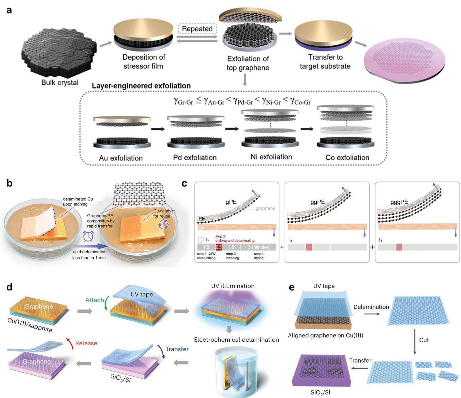
While the unique properties of monolayer 2D materials have been widely explored, growing attention has been devoted to their multilayer counterparts. In multilayer systems, the number of atomic layers and their stacking configurations play a decisive role in determining the electronic structure, interlayer coupling, optical response, and overall device performance. While the 2D materials family has expanded dramatically in recent years, graphene, h-BN, and TMDs (particularly MoS2) remain the most deeply studied systems due to their stable fabrication protocols and well-understood structure–property relationships. For example, bilayer and trilayer graphene (TLG) structures exhibit stacking-dependent bandgap tunability, unconventional superconductivity, and topological phenomena. Similarly, multilayer h-BN shows enhanced dielectric screening and has been shown to support sliding ferroelectricity under certain stacking orders. TMDs, such as MoS2 and WSe2, undergo a transition from direct to indirect bandgap with increasing layer number and demonstrate significantly improved carrier transport and thermal stability in multilayer form, enabling their integration in high-performance field-effect transistors, photodetectors, and neuromorphic devices. Achieving precise control over layer number and stacking order in these materials is thus of paramount importance, both for fundamental investigations and practical applications. However, this remains a significant challenge, as it requires atomic-level precision in the vertical assembly of van der Waals (vdW) layers while maintaining high crystallinity and clean interfaces. To address this, various fabrication strategies have been developed, which can be broadly classified into artificial assembly and direct growth methods.
Loading authentic research manuscript (Pages 1–5)...
FAN Aiqing, ZHANG Qing, WANG Yongshuai, LI Lin, WU Fan, GENG Dechao (2025). Recent advances in layer engineering and controllable fabrication of graphene, h-BN, and transition metal dichalcogenides. SCIENCE CHINA Materials. https://doi.org/10.1007/s40843-025-3656-9
Research & Educational Purpose Only: The translations, structured abstracts, analytical annotations, and data reports provided by SinoGreenTechare intended exclusively for academic research, internal corporate R&D, and educational benchmarking. They do not constitute formal engineering, chemical safety, legal, or professional advice.
Copyright & Intellectual Property Notice: Original copyright of the underlying source articles and experimental data remains with the respective authors, institutions, and original publishing journals. SinoGreenTech claims intellectual property only over its proprietary translations, analytical syntheses, and AEO structured enhancements in accordance with international fair use and academic citation principles.
Frequently Asked Questions
What are the primary failure mechanisms in multilayer TMD-based devices under electrical stress?
Under high current densities (>10^7 A/cm²) and prolonged operation, multilayer TMDs such as MoS2 can suffer from Joule heating-induced degradation, leading to sulfur vacancy migration and eventual breakdown. Encapsulation with h-BN and interface engineering can mitigate these effects, but long-term reliability data beyond 10^4 hours are still lacking.
How does the cost of CVD-grown multilayer 2D materials compare to legacy silicon-based technologies?
Current CVD growth of wafer-scale multilayer MoS2 costs approximately $100–$200 per 4-inch wafer, significantly higher than silicon ($10–$20 per wafer). However, for niche applications such as flexible electronics and quantum devices, the performance advantages may justify the premium. Scaling to 8-inch wafers and reducing precursor costs could bring parity by 2030.
What are the scalability bottlenecks for layer-by-layer assembly of 2D heterostructures?
The primary bottlenecks are transfer-induced contamination (polymer residues) and misalignment during stacking, which limit yield to <70% for 3-layer stacks. Automated robotic assembly with sub-micron alignment accuracy and clean transfer techniques (e.g., crack propagation) are essential for achieving >95% yield at wafer scale.
How does the interlayer twist angle affect the electronic properties of multilayer MoS2, and what is the optimal angle for device performance?
Twist angles near 0° or 60° yield aligned (3R or 2H) stacking with high mobility, while intermediate angles (e.g., 30°) create moiré superlattices that can induce flat bands and correlated insulating states. For high-performance transistors, aligned stacking is preferred, but for quantum applications, magic-angle twisted bilayer MoS2 (≈1.1°) shows superconductivity.
What are the current limitations in achieving uniform thickness over large areas for CVD-grown multilayer graphene?
CVD-grown multilayer graphene often exhibits thickness variations of ±1 layer over centimeter scales due to non-uniform carbon supply and substrate imperfections. This leads to inconsistent sheet resistance (e.g., 100–500 Ω/sq). Advanced control of gas flow and substrate surface treatment can reduce variation to <5%, but wafer-scale uniformity remains a challenge.
Related Chinese Research & Cross-Citations

Ammonium Vanadate Cathodes in Aqueous Zinc-Ion Batteries: Design Strategies and Research Progress
Aqueous zinc-ion batteries (AZIBs) offer a compelling combination of high safety, environmental compatibility, and abundant zinc resources, positioning them as viable candidates for grid-scale energy storage. Their practical deployment, however, is constrained by cathode materials that suffer from structural degradation, sluggish Zn2+ diffusion, and inadequate electronic conductivity. Ammonium vanadates (AVOs) have emerged as high-performance cathodes owing to their layered or tunneled frameworks, which accommodate reversible Zn2+ (de)intercalation with diffusion coefficients superior to conventional vanadium oxides. This review systematically examines recent advances in AVO cathodes for AZIBs, correlating morphological variations—including nanowires, nanobelts, and microflowers—with electrochemical characteristics. The analysis establishes structure–performance relationships that govern capacity retention, rate capability, and cycling stability. Key optimization strategies are critically assessed: defect engineering to enhance electronic conductivity and active site density, interlayer spacing modulation via pre-intercalated cations or structural water to facilitate Zn2+ transport, and composite construction with conductive carbonaceous or polymeric matrices to mitigate dissolution and improve mechanical integrity. Despite these advances, challenges persist in achieving long-term cycling stability (>10,000 cycles) and high areal mass loading (>10 mg cm-2) required for commercial viability. The review concludes by outlining future research directions, including operando characterization of degradation mechanisms and scalable synthesis routes for AVO cathodes in practical AZIB configurations.

Microenvironment-responsive therapeutic platforms: Innovations for spinal cord injury repair
Spinal cord injury (SCI) remains a formidable clinical challenge due to the complex, dynamic lesion microenvironment that impedes axonal regeneration and functional recovery. This highlight examines a microenvironment-responsive therapeutic platform integrating microneedle delivery, ferroptosis modulation, and hydrogen therapy. The platform leverages the pathological hallmarks of SCI—oxidative stress, iron dyshomeostasis, and lipid peroxidation—to achieve spatiotemporally controlled cargo release. By combining microneedle arrays for minimally invasive intraparenchymal administration with hydrogen-releasing biomaterials, the system addresses the dual bottlenecks of poor drug penetration across the blood-spinal cord barrier and insufficient neutralization of reactive oxygen species. Ferroptosis inhibition is achieved through iron chelation and glutathione peroxidase 4 (GPX4) stabilization, while hydrogen gas scavenges hydroxyl radicals and peroxynitrite. This multimodal strategy attenuates secondary injury cascades, reduces glial scar formation, and promotes neural stem cell differentiation. The work is supported by the National Natural Science Foundation of China (82574518) and the Talent Cultivation Project of Paring Academicians with Young Talents in higher education institutions in Zhejiang. The authors declare no conflict of interest. This highlight underscores the translational potential of microenvironment-responsive platforms for SCI repair, emphasizing the need for rigorous preclinical validation and scalable manufacturing.

Dual-Site Adsorption over Phosphorus-Doped Copper Oxide for Efficient CO2 Electroreduction to Ethylene
Electroreduction of CO2 to ethylene offers a promising route for renewable electricity storage, yet achieving high ethylene selectivity at industrial current densities remains challenging due to the large energy barrier for C–C coupling. Here, we report a “MOF-assisted in situ doping” strategy to introduce the oxophilic nonmetal phosphorus (P) into the copper oxide (CuO) lattice, constructing a localized Cu–P dual-site adsorption configuration for the key *OCCHO intermediate. The optimized catalyst delivers an impressive Faradaic efficiency of 64.6% for ethylene with a partial current density of 646 mA cm-2. Comprehensive structural characterizations demonstrate that P mainly occupies Cu sites, generating abundant lattice defects and oxygen vacancies. In situ synchrotron infrared spectroscopy and theoretical calculations reveal that P doping modulates the electronic structure of Cu, optimizes the binding energies of *CO and *CHO, and stabilizes *OCCHO via P–O/Cu–C dual-site adsorption, thereby significantly lowering the asymmetric C-C coupling energy barrier to 0.74 eV. This work highlights a dual-site microenvironment regulation strategy for CO2-to-ethylene electroreduction.

Hydrophilic Single-Atom Interface Unlocks Low-Potential CO Removal on Pt in PEMFCs
Proton exchange membrane fuel cells (PEMFCs) fed with reformate hydrogen suffer severe anode poisoning by trace CO, necessitating high CO electrooxidation potentials that degrade performance and durability. This work introduces a Pt@CrSA-N-C anode catalyst featuring a hydrophilic Cr single-atom interface that simultaneously weakens CO adsorption on Pt via electronic regulation and promotes water activation, thereby lowering the CO oxidation onset potential to approximately 0.13 V vs. RHE. The onset potential was determined by two independent methods: the first potential at which the background-corrected current exceeds 0 mA cm-2 during CO oxidation reaction tests in a three-electrode system, and the potential at which the forward scan current exceeds the N2 background current in CO-stripping voltammetry. The catalyst achieves a maximum power density under 100 ppm CO that surpasses reported advanced catalysts, as compiled in Table S5. Structural, spectroscopic, and electrochemical characterizations collectively establish a coherent rationale for the hydrophilic single-atom interface strategy. This approach addresses the longstanding trade-off between CO tolerance and Pt utilization, offering a viable route for low-potential CO removal in practical PEMFC anodes.

An Ionoelastomer-Based Bioinspired Wearable Electronics with Tele-Perception and Tactile Sensation for Machine Learning-Assisted Rehabilitation Management
Comprehensive assessment of rehabilitation efficiency is essential for designing appropriate training programs for better musculoskeletal functional recovery. Existing contact-receptor-dependent rehabilitation assessment systems mostly focus on assessing the restoration of muscle function by evaluating grip strength or joint flexion angle; however, parameters reflecting neuromuscular synergistic function are always overlooked. Herein, we develop an ionoelastomer-based soft artificial electroreceptor (SAER) that integrates tele-perception and tactile sensation to track the rehabilitation process, collecting signals related to approaching speed and grip strength sequentially. The SAER uses polyurethane ionoelastomer incorporated with quasi-solid conductive salt as the electric field receptor, and is integrated on a rehabilitation-training ball after assembly to establish an untethered detection device; this enables the remote capture of hand approaching parameter within a 9 cm range, followed by the quantification of grip strength when contacting and grasping. Furthermore, a data-driven assessment system is established by integrating machine learning, which accurately classifies rehabilitation efficiency into six levels; it supports for rehabilitation evaluation and training programs adjustment. Overall, the SAER-based rehabilitation management system establishes a paradigm that synergistically evaluating parameters corresponding to neuromuscular functional restoration and holds strong potential for home-based active rehabilitation for minimizing dependence on frequent clinical supervision.

Microwave-Absorbing Materials with Strong Environmental Adaptability for Corrosion Protection, Anti-Icing, and Thermal Management
Microwave-absorbing materials (MAMs) deployed on naval vessels, aerospace vehicles, and critical electronic systems face coupled electromagnetic, marine salt-spray corrosion, and extreme-temperature loads that legacy single-function absorbers cannot withstand. This review consolidates progress on three environmentally adaptive MAM classes: corrosion-protective, anti-icing, and thermal-management absorbers. The electromagnetic loss and impedance-matching fundamentals are first established, then the synergistic mechanisms, design strategies, and characterization protocols for each class are examined against representative material systems and their measured performance. The analysis identifies a shared design logic—multiscale hierarchical architecture, interfacial polarization engineering, and multifunctional phase integration—while distinguishing the divergent protection mechanisms: barrier and passivation effects for corrosion, surface-energy and latent-heat regulation for anti-icing, and phonon–electron transport decoupling for thermal management. Persistent bottlenecks include the trade-off between impedance matching and protective-layer density, the absence of standardized coupled-field test protocols, and the scarcity of long-term salt-spray and thermal-cycling durability data. Future directions are delineated: intelligent self-adaptive absorbers, multiphysics-coupled simulation frameworks, and environmentally benign multifunctional integration. The review provides a theoretical and technical basis for the design, construction, and engineering scale-up of next-generation high-performance absorbers for aerospace, electronic, and marine equipment.